1. 什么是PPI和DPPI?
- PPI,英文全称是Programmable Peripheral Interconnect;
- DPPI,英文全称是Distributed Programmable Peripheral Interconnect。
PPI是nRF52系列芯片的一个外设,从nRF53系列开始,使用DPPI代替了PPI。PPI和DPPI的设计目的是相同的,都提供了一种机制,让某个外设的事件可以触发另一个外设的任务,让一个外设直接控制另一个外设成为可能,从而减少了CPU的参与,和DMA有异曲同工之效。比如,我们可以用timer定时器去触发一个ADC采样,这样就不需要CPU执行指令去触发采样了。所谓编程(Programmable),就是指可以通过配置寄存器,将不同外设的事件和任务建立关联。
2. 什么是事件(event)和任务(task)?
说到PPI和DPPI就绕不过事件和任务。那么这个事件和任务又是什么呢?学习过MCU的同学都知道外设(Peripheral)都会有与之对应的控制寄存器和状态寄存器,而我们Nordic的控制寄存器和状态寄存器的设计有些与众不同。我们将控制寄存器的控制逻辑做了细分,将每一个控制逻辑都具体成了一个任务,一个任务就对应一个任务寄存器。同样,将状态寄存器的状态也做了细分,将每一个不同的状态都具体成了一个事件,一个事件就对应一个事件寄存器。
以UARTE模块为例,它的task和event寄存器如下:
| Register |
Offset |
Description |
| TASKS_STARTRX |
0x000 |
Start UART receiver |
| TASKS_STOPRX |
0x004 |
Stop UART receiver |
| TASKS_STARTTX |
0x008 |
Start UART transmitter |
| TASKS_STOPTX |
0x00C |
Stop UART transmitter |
| TASKS_FLUSHRX |
0x02C |
Flush RX FIFO into RX buffer |
|
... |
|
| EVENTS_CTS |
0x100 |
CTS is activated (set low). Clear To Send. |
| EVENTS_NCTS |
0x104 |
CTS is deactivated (set high). Not Clear To Send. |
| EVENTS_RXDRDY |
0x108 |
Data received in RXD (potentially not yet transferred to Data RAM) |
| EVENTS_ENDRX |
0x110 |
Receive buffer is filled up |
| EVENTS_TXDRDY |
0x11C |
Data sent from TXD |
| EVENTS_ENDTX |
0x120 |
Last TX byte transmitted |
| EVENTS_ERROR |
0x124 |
Error detected |
| EVENTS_RXTO |
0x144 |
Receiver timeout |
| EVENTS_RXSTARTED |
0x14C |
UART receiver has started |
| EVENTS_TXSTARTED |
0x150 |
UART transmitter has started |
| EVENTS_TXSTOPPED |
0x158 |
Transmitter stopped |
3. 什么是通道(Channel)?
通道可以想象成一个管道,管道的输入端关联event寄存器,管道的输出端关联task寄存器。管道上有开关,当开关被打开时(channel enable),event寄存器如果有信号,就能触发管道另一头的task寄存器,从而触发task寄存器对应的控制逻辑。PPI和DPPI的主要区别是:通道与event寄存器和task寄存器建立关联的机制不同。PPI的机制决定了一个通道只能关联一个event和一个task,即只能一对一(一个event触发一个task),利用fork机制可以做到一对二(一个event触发两个task)。DPPI的一个通道可以和多个task和event做关联,能做到多对多(多个event触发多个task)。另外,通道还有自己的管理机制,还可以分组管理。PPI和DPPI的通道管理机制是相同的。
4.PPI框图
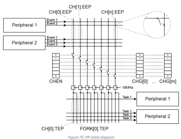
-
EEP是event end point的缩写;TEP是task end point的缩写。每一个通道都有自己的EEP和TEP寄存器。
-
CH[i].EEP是一个配置寄存器,负责存储event register 地址,使外设的event与通道i(CH[i])建立关联。
-
CH[i].TEP也是一个配置寄存器,负责存储task register 地址,使外设的task与通道i (CH[i])建立关联。
-
PPI允许一个event或task和多个通道建立关联。即不同的通道里可以写入同一个event或task地址。但一个通道只能和一个event建立关联,因为某个通道i对应的CH[i].EEP里只能写入一个地址。Task比较特殊,因为有FORK[i].TEP的存在,所以CH[i].TEP和FORK[i].TEP可以写入两个不同的task register地址,实现一对二。FORK功能只存在于PPI,DPPI没有FORK功能。
-
接入同一个通道的event和task可以形成通路,为event触发task逻辑创造条件。
-
CHEN, CHENSET, CHENCLR和CHG[m]则是用来管理这些通道(enable and disable the channels)是否使能。
-
0-19通道可以任意配置;20-31通道的task和event是固定的,不能配置。
| Instance |
Channel |
Number of channels |
| PPI |
0-19 |
20 |
| PPI (fixed) |
20-31 |
12 |
| Channel |
EEP |
TEP |
| 20 |
TIMER0->EVENTS_COMPARE[0] |
RADIO->TASKS_TXEN |
| 21 |
TIMER0->EVENTS_COMPARE[0] |
RADIO->TASKS_RXEN |
| 22 |
TIMER0->EVENTS_COMPARE[1] |
RADIO->TASKS_DISABLE |
| 23 |
RADIO->EVENTS_BCMATCH |
AAR->TASKS_START |
| 24 |
RADIO->EVENTS_READY |
CCM->TASKS_KSGEN |
| 25 |
RADIO->EVENTS_ADDRESS |
CCM->TASKS_CRYPT |
| 26 |
RADIO->EVENTS_ADDRESS |
TIMER0->TASKS_CAPTURE[1] |
| 27 |
RADIO->EVENTS_END |
TIMER0->TASKS_CAPTURE[2] |
| 28 |
RTC0->EVENTS_COMPARE[0] |
RADIO->TASKS_TXEN |
| 29 |
RTC0->EVENTS_COMPARE[0] |
RADIO->TASKS_RXEN |
| 30 |
RTC0->EVENTS_COMPARE[0] |
TIMER0->TASKS_CLEAR |
| 31 |
RTC0->EVENTS_COMPARE[0] |
TIMER0->TASKS_START |
CH[n].EEP (n=0..19)
Address offset: 0x510 + (n × 0x8)
Channel n event endpoint

| ID |
Access |
Field |
ValueID |
Value |
Description |
| A |
RW |
EEP |
|
|
Pointer to event register. Accepts only addresses to registers from the Event group. |
CH[n].TEP (n=0..19)
Address offset: 0x514 + (n × 0x8)
Channel n task endpoint
| ID |
Access |
Field |
ValueID |
Value |
Description |
| A |
RW |
TEP |
|
|
Pointer to task register. Accepts only addresses to registers from the Task group. |
FORK[n].TEP (n=0..19, 20..31)
Address offset: 0x910 + (n × 0x4)
Channel n task endpoint

| ID |
Access |
Field |
ValueID |
Value |
Description |
| A |
RW |
TEP |
|
|
Pointer to task register. |
5.DPPI框图
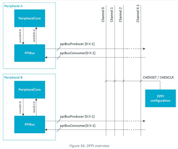
- 所有外围设备都含有一系列的任务订阅寄存器和事件发布寄存器(每个task寄存器对应一个订阅( subscribe)寄存器;每个event寄存器对应一个发布(publish)寄存器)。(订阅和发布寄存器取代了PPI中EEP和TEP寄存器的功能)
- 发布和订阅的对象是通道(channel)
- 同一个通道可以被不同的事件发布,被不同的任务订阅,达到多对多的效果。
- 以下是ADC模块的task,event,subscribe task,publish event寄存器。
| Register |
Offset |
Description |
| TASKS_START |
0x000 |
Start the ADC and prepare the result buffer in RAM |
| TASKS_SAMPLE |
0x004 |
Take one ADC sample, if scan is enabled all channels are sampled |
| TASKS_STOP |
0x008 |
Stop the ADC and terminate any ongoing conversion |
| TASKS_CALIBRATEOFFSET |
0x00C |
Starts offset auto-calibration |
| SUBSCRIBE_START |
0x080 |
Subscribe configuration for task START |
| SUBSCRIBE_SAMPLE |
0x084 |
Subscribe configuration for task SAMPLE |
| SUBSCRIBE_STOP |
0x088 |
Subscribe configuration for task STOP |
| SUBSCRIBE_CALIBRATEOFFSET |
0x08C |
Subscribe configuration for task CALIBRATEOFFSET |
| EVENTS_STARTED |
0x100 |
The ADC has started |
| EVENTS_END |
0x104 |
The ADC has filled up the Result buffer |
| EVENTS_DONE |
0x108 |
A conversion task has been completed. Depending on the mode, multiple conversions might be needed for a result to be transferred to RAM. |
| EVENTS_RESULTDONE |
0x10C |
A result is ready to get transferred to RAM |
| EVENTS_CALIBRATEDONE |
0x110 |
Calibration is complete |
| EVENTS_STOPPED |
0x114 |
The ADC has stopped |
| EVENTS_CH[n].LIMITH |
0x118 |
Last results is equal or above CH[n].LIMIT.HIGH |
| EVENTS_CH[n].LIMITL |
0x11C |
Last results is equal or below CH[n].LIMIT.LOW |
| PUBLISH_STARTED |
0x180 |
Publish configuration for event STARTED |
| PUBLISH_END |
0x184 |
Publish configuration for event END |
| PUBLISH_DONE |
0x188 |
Publish configuration for event DONE |
| PUBLISH_RESULTDONE |
0x18C |
Publish configuration for event RESULTDONE |
| PUBLISH_CALIBRATEDONE |
0x190 |
Publish configuration for event CALIBRATEDONE |
| PUBLISH_STOPPED |
0x194 |
Publish configuration for event STOPPED |
| PUBLISH_CH[n].LIMITH |
0x198 |
Publish configuration for event CH[n].LIMITH |
| PUBLISH_CH[n].LIMITL |
0x19C |
Publish configuration for event CH[n].LIMITL |
6. 通道管理和组(group)
CHENSET
Address offset: 0x504
Channel enable set register
Note: Read: Reads value of CH[i] field in CHEN register

| ID |
Access |
Field |
ValueID |
Value |
Description |
| A-f |
RW |
CH[i] (i=0..31) |
|
|
Channel i enable set register. Writing '0' has no effect. |
|
|
|
Disabled |
0 |
Read: channel disabled |
|
|
|
Enabled |
1 |
Read: channel enabled |
|
|
|
Set |
1 |
Write: Enable channel |
CHENCLR
Address offset: 0x508
Channel enable clear register
Note: Read: Reads value of CH[i] field in CHEN register

| ID |
Access |
Field |
ValueID |
Value |
Description |
| A-f |
RW |
CH[i] (i=0..31) |
|
|
Channel i enable set register. Writing '0' has no effect. |
|
|
|
Disabled |
0 |
Read: channel disabled |
|
|
|
Enabled |
1 |
Read: channel enabled |
|
|
|
Set |
1 |
Write: Enable channel |
- CHENSET和CHENCLR寄存器用于设置通道,如果要读取通道的状态,需要读取CHEN寄存器。
CHEN
Address offset: 0x500
Channel enable register
| ID |
Access |
Field |
ValueID |
Value |
Description |
| A-f |
RW |
CH[i] (i=0..31) |
|
|
Channel i enable set register. Writing '0' has no effect. |
|
|
|
Disabled |
0 |
Read: channel disabled |
|
|
|
Enabled |
1 |
Read: channel enabled |
|
|
|
Set |
1 |
Write: Enable channel |
- 不同的通道可以分配到一个组里。一共支持6个组。CHG[n](n=0..5)寄存器有32bit,每一个bit位对应一个通道号,如果相应的bit位被置“1”,那么这个通道就被分配到了当前的组中。
CHG[n] (n=0..5)
Address offset: 0x800 + (n x 0x4)
Channel group n
Note: Writes to this register are ignored if either SUBSCRIBE_CHG[n].EN or SUBSCRIBE_CHG[n].DIS are enabled
| ID |
Access |
Field |
ValueID |
Value |
Description |
| A-f |
RW |
CH[i] (i=0..31) |
|
|
Include or exclude channel i |
|
|
|
Excluded |
0 |
Exclude |
|
|
|
Included |
1 |
Include |
- 每一个组都有两个task寄存器,一个task(TASKS_CHG[n].EN)控制组使能,另一个task (TASKS_CHG[n].DIS)控制组禁用。有了task,那么它们也可以通过PPI/DPPI的机制,被别的event触发。当TASKS_CHG[n].EN被触发,同一组内所有的通道被使能;当TASKS_CHG[n].DIS被触发,同一组内所有的通道被禁用。
TASKS_CHG[n].EN (n=0..5)
Address offset: 0x000 + (n x 0x8)
Enable channel group n

| ID |
Access |
Field |
ValueID |
Value |
Description |
| A |
W |
EN |
|
|
Enable channel group n |
|
|
|
Trigger |
1 |
Trigger task |
TASKS_CHG[n].DIS (n=0..5)
Address offset: 0x004 + (n x 0x8)
Disable channel group n
| ID |
Access |
Field |
ValueID |
Value |
Description |
| A |
W |
DIS |
|
|
Disable channel group n |
|
|
|
Trigger |
1 |
Trigger task |
7. PPI和DPPI的驱动资源及使用流程
- PPI 驱动位于modules\hal\nordic\nrfx\drivers\src\nrfx_ppi.c;DPPI驱动位于modules\hal\nordic\nrfx\drivers\src\nrfx_dppi.c
- 为了兼容PPI和DPPI,还设计了辅助层(Helper layer:modules\hal\nordic\nrfx\helpers\nrfx_gppi.h) 提供 PPI 和 DPPI 驱动的通用功能。辅助层直接调用PPI和DPPI的驱动程序,使用辅助层时,需要考虑到PPI 和 DPPI 接口在应用时的明显差异。
- PPI和DPPI的使用流程相同,都很简单:
1)分配(申请)通道
2)对于PPI,通道两端分别关联task和event;对于DPPI,task(Subscribe)和event(Publish)端关联通道
3)使能通道
8. PPI和DPPI配置代码示例
1)Timer COMPARE0 EVENT产生的时候触发ADC采样。按下button1启动timer,端口输出低电平,按下button2停止timer,端口输出高电平。下面列举了PPI多通道,以及FORK使用的配置代码。
status = nrfx_ppi_channel_alloc(&m_timer_saadc_ppi_channel);
NRFX_ASSERT(status == NRFX_SUCCESS);
status = nrfx_ppi_channel_assign(m_timer_saadc_ppi_channel,
nrfx_timer_event_address_get(&m_sample_timer, NRF_TIMER_EVENT_COMPARE0),
nrf_saadc_task_address_get(NRF_SAADC, NRF_SAADC_TASK_SAMPLE));
NRFX_ASSERT(status == NRFX_SUCCESS);
status = nrfx_ppi_channel_alloc(&m_button0_timer_ppi_channel);
NRFX_ASSERT(status == NRFX_SUCCESS);
status = nrfx_ppi_channel_assign(m_button0_timer_ppi_channel,
nrfx_gpiote_in_event_addr_get(INPUT_PIN_0),
nrf_timer_task_address_get(m_sample_timer.p_reg, NRF_TIMER_TASK_START));
NRFX_ASSERT(status == NRFX_SUCCESS);
status = nrfx_ppi_channel_fork_assign(m_button0_timer_ppi_channel,
nrfx_gpiote_clr_task_addr_get(OUTPUT_PIN));
NRFX_ASSERT(status == NRFX_SUCCESS);
status = nrfx_ppi_channel_alloc(&m_button1_timer_ppi_channel);
NRFX_ASSERT(status == NRFX_SUCCESS);
status = nrfx_ppi_channel_assign(m_button1_timer_ppi_channel,
nrfx_gpiote_in_event_addr_get(INPUT_PIN_1),
nrf_timer_task_address_get(m_sample_timer.p_reg, NRF_TIMER_TASK_STOP));
NRFX_ASSERT(status == NRFX_SUCCESS);
status = nrfx_ppi_channel_fork_assign(m_button1_timer_ppi_channel,
nrfx_gpiote_set_task_addr_get(OUTPUT_PIN));
NRFX_ASSERT(status == NRFX_SUCCESS);
2)Timer COMPARE0 EVENT产生的时候触发ADC采样。按下button1启动timer,端口输出低电平,按下button2停止timer,端口输出高电平。下面列举了DPPI多通道使用的配置代码。
status = nrfx_dppi_channel_alloc(&m_timer_saadc_dppi_channel);
NRFX_ASSERT(status == NRFX_SUCCESS);
nrf_timer_publish_set(m_sample_timer.p_reg, NRF_TIMER_EVENT_COMPARE0,
m_timer_saadc_dppi_channel);
nrf_saadc_subscribe_set(NRF_SAADC, NRF_SAADC_TASK_SAMPLE, m_timer_saadc_dppi_channel);
status = nrfx_dppi_channel_alloc(&m_button0_timer_dppi_channel);
NRFX_ASSERT(status == NRFX_SUCCESS);
nrf_gpiote_publish_set(NRF_GPIOTE, nrfx_gpiote_in_event_get(INPUT_PIN_0),
m_button0_timer_dppi_channel);
nrf_gpiote_subscribe_set(NRF_GPIOTE,nrfx_gpiote_clr_task_addr_get(OUTPUT_PIN),m_button0_timer_dppi_channel);
NRFX_ASSERT(status == NRFX_SUCCESS);
nrf_timer_subscribe_set(m_sample_timer.p_reg, NRF_TIMER_TASK_START, m_button0_timer_dppi_channel);
NRFX_ASSERT(status == NRFX_SUCCESS);
status = nrfx_dppi_channel_alloc(&m_button1_timer_dppi_channel);
NRFX_ASSERT(status == NRFX_SUCCESS);
nrf_gpiote_publish_set(NRF_GPIOTE, nrfx_gpiote_in_event_get(INPUT_PIN_1),
m_button1_timer_dppi_channel);
nrf_gpiote_subscribe_set(NRF_GPIOTE,nrfx_gpiote_set_task_addr_get(OUTPUT_PIN),m_button1_timer_dppi_channel);
NRFX_ASSERT(status == NRFX_SUCCESS);
nrf_timer_subscribe_set(m_sample_timer.p_reg, NRF_TIMER_TASK_STOP, m_button1_timer_dppi_channel);
NRFX_ASSERT(status == NRFX_SUCCESS);
3)组(group)的使用代码示例。使用timer,gpiote,dppi输出固定周期的波形。只有在COMPARE2 EVENT发生的时候,将输出电平置高;在COMPARE3 EVENT发生的时候,将输出电平置低。第一次产生COMPARE1 EVENT的时候,触发了timer clear的task, timer重新开始计数,那么COMPARE0 EVENT就不会发生了。 COMPARE1 EVENT还触发了group disable task。那么,下一个COMPARE1 EVENT就不会触发timer clear task了,因为这个channel被disable了。 COMPARE1 EVENT发生后, COMPARE0 EVENT会接着发生。在COMPARE0 EVENT产生的中断处理里面,通过group的控制函数,又将channel使能了。那么,COMPARE1 EVENT,又能触发了timer clear task,循环上面的动作。输出波形如下:

#define PERIOD (20*16000)
#define SHORT_PERIOD (10*16000)
#define OFFSET 1
#define PULSE_WIDTH (5*16000)
static void timer_init(void)
{
    nrfx_timer_config_t timer_config = NRFX_TIMER_DEFAULT_CONFIG;
    timer_config.frequency = NRF_TIMER_FREQ_125kHz;
    timer_config.bit_width = NRF_TIMER_BIT_WIDTH_32;
    nrfx_timer_init(&timer, &timer_config, timer_handler);
    nrfx_timer_compare(&timer, NRF_TIMER_CC_CHANNEL0, PERIOD, true);
    nrf_timer_shorts_enable(timer.p_reg, NRF_TIMER_SHORT_COMPARE0_CLEAR_MASK);
    nrfx_timer_compare(&timer, NRF_TIMER_CC_CHANNEL1, SHORT_PERIOD, true);
    nrfx_timer_compare(&timer, NRF_TIMER_CC_CHANNEL2, OFFSET, false);
    nrfx_timer_compare(&timer, NRF_TIMER_CC_CHANNEL3, OFFSET + PULSE_WIDTH, false);

    IRQ_CONNECT(TIMER0_IRQn, NRFX_TIMER_DEFAULT_CONFIG_IRQ_PRIORITY - 1,
        nrfx_timer_0_irq_handler, NULL, 0);

    configure_one_time_clear();
    nrfx_timer_enable(&timer);

}
static void timer_handler(nrf_timer_event_t event_type, void *p_context)
{
if (event_type == NRF_TIMER_EVENT_COMPARE0) {
printk("0");
nrfx_dppi_group_enable(group_ch);
}
if (event_type == NRF_TIMER_EVENT_COMPARE1) {
printk("1");
}
}
- DPPI分配组,分配通道,关联通道配置COMPARE1 EVENT触发timer clear,加入组,配置COMPARE1 EVENT触发group disable task。然后使能通道。
static void configure_one_time_clear(void)
{
nrfx_dppi_group_alloc(&group_ch);
nrfx_dppi_channel_alloc(&channel_ch);
nrf_timer_publish_set(timer.p_reg, NRF_TIMER_EVENT_COMPARE1, channel_ch);
nrf_timer_subscribe_set(timer.p_reg, NRF_TIMER_TASK_CLEAR, channel_ch);
nrfx_dppi_channel_include_in_group(channel_ch, group_ch);
nrf_dppi_subscribe_set(NRF_DPPIC, nrf_dppi_group_disable_task_get(group_ch), channel_ch);
nrfx_dppi_channel_enable(channel_ch);
}
- DPPI分配通道,配置COMPARE2 EVENT触发output ‘H’,使能通道;DPPI分配通道,配置COMPARE3 EVENT触发output ‘L’,使能通道。
nrfx_gpiote_out_init(OUTPUT_PIN, &out_config);
nrfx_gpiote_out_task_enable(OUTPUT_PIN);

uint8_t channel;
nrfx_dppi_channel_alloc(&channel);
nrf_timer_publish_set(timer.p_reg, NRF_TIMER_EVENT_COMPARE2, channel);
nrf_gpiote_subscribe_set(
        NRF_GPIOTE,
        nrfx_gpiote_set_task_get(OUTPUT_PIN),
        channel);
nrfx_dppi_channel_enable(channel);

nrfx_dppi_channel_alloc(&channel);
nrf_timer_publish_set(timer.p_reg, NRF_TIMER_EVENT_COMPARE3, channel);
nrf_gpiote_subscribe_set(
        NRF_GPIOTE,
        nrfx_gpiote_clr_task_get(OUTPUT_PIN),
        channel);
nrfx_dppi_channel_enable(channel);
上述完整代码可在百度网盘下载